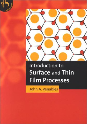
John A. Venables9780521785006, 0521785006, 0521624606
Table of contents :
Contents……Page 3
Preface……Page 9
1.1.1 Thermodynamic potentials and the dividing surface……Page 15
1.1.2 Surface tension and surface energy……Page 17
1.2 Surface energies and the Wulff theorem……Page 18
1.2.2 The terrace–ledge–kink model……Page 19
1.2.3 Wulff construction and the forms of small crystals……Page 21
1.3 Thermodynamics versus kinetics……Page 23
1.3.1 Thermodynamics of the vapor pressure……Page 25
1.3.2 The kinetics of crystal growth……Page 29
1.4.1 Overview……Page 33
1.4.2 General comments and notation……Page 34
1.4.3 Examples of (1 x 1) structures……Page 36
1.4.4 Si(001) (2 x 1) and related semiconductor structures……Page 38
1.4.5 The famous 7 x 7 stucture of Si(111)……Page 41
1.4.7 Polar semiconductors, such as GaAs(111)……Page 42
1.5.2 Electron affinity, x and ionization potential Φ……Page 44
1.5.3 Surface states and related ideas……Page 45
1.5.6 The image force……Page 46
Problems for chapter 1……Page 47
2.1.1 Arrival rate of atoms at a surface……Page 50
2.1.3 The mean free path, λ……Page 51
2.1.4 The monolayer arrival time, τ……Page 52
2.2.1 System volumes, leak rates and pumping speeds……Page 53
2.2.2 The idea of conductance……Page 55
2.3.1 Introduction: sources of information……Page 56
2.3.2 Types of pump……Page 57
2.3.3 Chambers, tube and flange sizes……Page 58
2.3.4 Choice of materials……Page 59
2.3.5 Pressure measurement and gas composition……Page 60
2.4.1 Cleaning and sample preparation……Page 61
2.4.2 Procedures for in situ experiments……Page 64
2.4.3 Sample transfer devices……Page 65
2.4.4 From laboratory experiments to production processes……Page 66
2.5.2 Thermal evaporation and the uniformity of deposits……Page 68
2.5.4 Sputtering and ion beam assisted deposition……Page 71
2.5.5 Chemical vapor deposition techniques……Page 73
Problems for chapter 2……Page 74
3.1.1 Surface techniques as scattering experiments……Page 77
3.1.2 Reasons for surface sensitivity……Page 78
3.1.3 Microscopic examination of surfaces……Page 79
3.1.4 Acronyms……Page 83
3.2.1 LEED……Page 84
3.2.2 RHEED and THEED……Page 86
3.2.3 Elastic, quasi-elastic and inelastic scattering……Page 88
3.3.1 Electron spectroscopic techniques……Page 90
3.3.2 Photoelectron spectroscopies: XPS and UPS……Page 93
3.3.3 Auger electron spectroscopy: energies and atomic physics……Page 95
3.3.4 AES, XPS and UPS in solids and at surfaces……Page 98
3.4.1 General equation describing quantification……Page 102
3.4.2 Ratio techniques……Page 106
3.5.1 Scanning electron and Auger microscopy……Page 109
3.5.2 Auger and image analysis of ‘real world’ samples……Page 112
3.5.3 Towards the highest spatial resolution: (a) SEM/STEM……Page 114
3.5.4 Towards the highest spatial resolution: (b) scanned probe microscopy-spectroscopy……Page 118
Problems, talks and projects for chapter 3……Page 119
4.1 Chemi- and physisorption……Page 122
4.2.2 Localized adsorption: the Langmuir adsorption isotherm……Page 123
4.2.3 The two-dimensional adsorbed gas: Henry law adsorption……Page 124
4.2.4 Interactions and vibrations in higher density adsorbates……Page 127
4.3 Phase diagrams and phase transitions……Page 128
4.3.1 Adsorption in equilibrium with the gas phase……Page 129
4.3.2 Adsorption out of equilibrium with the gas phase……Page 132
4.4.1 Thermodynamic information from single surface techniques……Page 133
4.4.2 The crystallography of monolayer solids……Page 134
4.4.3 Melting in two dimensions……Page 138
4.4.4 Construction and understanding of phase diagrams……Page 139
4.5.1 Phases and phase transitions of the lattice gas……Page 142
4.5.2 The Newns–Anderson model and beyond……Page 144
4.5.3 Chemisorption: the first stages of oxidation……Page 147
4.5.4 Chemisorption and catalysis: macroeconomics, macromolecules and microscopy……Page 149
Problems and projects for chapter 4……Page 155
5.1.1 Why are we studying epitaxial growth?……Page 158
5.1.3 Growth modes and adsorption isotherms……Page 159
5.1.4 Nucleation barriers in classical and atomistic models……Page 161
5.2.1 Rate equations, controlling energies, and simulations……Page 163
5.2.2 Elements of rate equation models……Page 164
5.2.3 Regimes of condensation……Page 166
5.2.4 General equations for the maximum cluster density……Page 168
5.2.5 Comments on individual treatments……Page 169
5.3.1 Microscopy of island growth: metals on alkali halides……Page 171
5.3.2 Metals on insulators: checks and complications……Page 173
5.3.3 Defect-induced nucleation on oxides and fluorides……Page 175
5.4.1 In situ UHV SEM and LEEM of metals on metals……Page 179
5.4.2 FIM studies of surface diffusion on metals……Page 181
5.4.3 Energies from STM and other techniques……Page 183
5.5.1 Steps as one-dimensional sinks……Page 188
5.5.2 Steps as sources: diffusion and Ostwald ripening……Page 190
5.5.3 Interdiffusion in magnetic multilayers……Page 193
Problems and projects for chapter 5……Page 195
6.1.1 Free electron models and density functionals……Page 198
6.1.2 Beyond free electrons: work function, surface structure and energy……Page 204
6.1.3 Values of the work function……Page 207
6.1.4 Values of the surface energy……Page 210
6.2.1 Thermionic emission……Page 214
6.2.2 Cold field emission……Page 216
6.2.3 Adsorption and diffusion: FES, FEM and thermal field emitters……Page 220
6.2.4 Secondary electron emission……Page 221
6.3.1 Symmetry, symmetry breaking and phase transitions……Page 224
6.3.2 Anisotropic interactions in 3D and ‘2D’ magnets……Page 225
6.3.3 Magnetic surface techniques……Page 227
6.3.4 Theories and applications of surface magnetism……Page 232
Problems and projects for chapter 6……Page 238
7.1.1 Bonding in diamond, graphite, Si, Ge, GaAs, etc…….Page 241
7.1.2 Simple concepts versus detailed computations……Page 243
7.1.3 Tight-binding pseudopotential and ab initio models……Page 244
7.2.1 GaAs(110), a charge-neutral surface……Page 246
7.2.2 GaAs(111), a polar surface……Page 248
7.2.3 Si and Ge(111): why are they so different?……Page 249
7.2.4 Si, Ge and GaAs(001), steps and growth……Page 253
7.3.1 Thermodynamic and elasticity studies of surfaces……Page 256
7.3.2 Growth on Si(001)……Page 259
7.3.3 Strained layer epitaxy: Ge/Si(001) and Si/Ge(001)……Page 263
7.3.4 Growth of compound semiconductors……Page 266
Further reading for chapter 7……Page 270
Problems and projects for chapter 7……Page 271
8.1.1 Band bending and rectifying contacts at semiconductor surfaces……Page 274
8.1.2 Simple models of the depletion region……Page 277
8.1.3 Techniques for analyzing semiconductor interfaces……Page 279
8.2.1 Origins of Schottky barrier heights……Page 284
8.2.2 Semiconductor heterostructures and band offsets……Page 286
8.2.3 Opto-electronic devices and ‘band-gap engineering’……Page 288
8.2.4 Modulation and δ-doping, strained layers, quantum wires and dots……Page 293
8.3 Conduction processes in thin film devices……Page 294
8.3.1 Conductivity, resistivity and the relaxation time……Page 295
8.3.2 Scattering at surfaces and interfaces in nanostructures……Page 296
8.3.3 Spin dependent scattering and magnetic multilayer devices……Page 298
8.4.1 Synthetic chemistry and manufacturing: the case of Si–Ge–C……Page 303
8.4.2 Chemical routes to opto-electronics and/or nano-magnetics……Page 305
8.4.3 Nanotubes and the future of flat panel TV……Page 307
8.4.4 Combinatorial materials development and analysis……Page 308
Further reading for chapter 8……Page 309
9.1 Electromigration and other degradation effects in nanostructures……Page 311
9.2 What do the various disciplines bring to the table?……Page 313
9.3 What has been left out: future sources of information……Page 315
Appendix A Bibliography……Page 317
Appendix B List of acronyms……Page 320
Appendix C Units and conversion factors……Page 323
Appendix D Resources on the web or CD-ROM……Page 326
Appendix E Useful thermodynamic relationships……Page 328
Appendix F Conductances and pumping speeds, C and S……Page 332
Appendix G Materials for use in ultra-high vacuum……Page 334
Appendix H UHV component cleaning procedures……Page 337
Appendix J An outline of local density methods……Page 340
Appendix K An outline of tight binding models……Page 342
References……Page 345
B……Page 377
D……Page 378
E……Page 379
J……Page 380
M……Page 381
P……Page 382
S……Page 383
T……Page 385
X……Page 386


Reviews
There are no reviews yet.