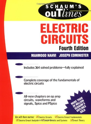
Mahmood Nahvi, Joseph Edminister9780071393072, 0071393072
Table of contents :
TeamLiB……Page 1
Cover……Page 2
Contents……Page 7
1.2 FORCE, WORK, AND POWER……Page 13
1.3 ELECTRIC CHARGE AND CURRENT……Page 14
1.4 ELECTRIC POTENTIAL……Page 15
1.6 CONSTANT AND VARIABLE FUNCTIONS……Page 16
2.1 PASSIVE AND ACTIVE ELEMENTS……Page 19
2.2 SIGN CONVENTIONS……Page 20
2.3 VOLTAGE- CURRENT RELATIONS……Page 21
2.4 RESISTANCE……Page 22
2.5 INDUCTANCE……Page 23
2.7 CIRCUIT DIAGRAMS……Page 24
2.8 NONLINEAR RESISTORS……Page 25
3.2 KIRCHHOFF¡¯S VOLTAGE LAW……Page 36
3.4 CIRCUIT ELEMENTS IN SERIES……Page 37
3.5 CIRCUIT ELEMENTS IN PARALLEL……Page 38
3.7 CURRENT DIVISION……Page 40
3.3 Find the current I for the circuit shown in Fig. 3- 9…….Page 41
3.5 Determine the equivalent inductance of the three parallel inductances shown in Fig. 3- 11…….Page 42
3.7 The circuit shown in Fig. 3- 13 is a voltage divider, also called an attenuator. When it is a single……Page 43
3.8 Find all branch currents in the network shown in Fig. 3- 14( a)…….Page 44
4.1 THE BRANCH CURRENT METHOD……Page 49
4.3 MATRICES AND DETERMINANTS……Page 50
4.4 THE NODE VOLTAGE METHOD……Page 52
4.5 INPUT AND OUTPUT RESISTANCES……Page 53
4.7 NETWORK REDUCTION……Page 54
4.8 SUPERPOSITION……Page 56
4.9 THE VENIN¡¯S AND NORTON¡¯S THEOREMS……Page 57
4.1 Use branch currents in the network shown in Fig. 4- 17 to . nd the current supplied by the 60- V……Page 59
4.2 Solve Problem 4.1 by the mesh current method…….Page 60
4.6 Solve Problem 4.1 by use of the loop currents indicated in Fig. 4- 20…….Page 61
4.7 Write the mesh current matrix equation for the network of Fig. 4- 21 by inspection, and solve for……Page 62
4.9 For the network shown in Fig. 4- 23, . nd Vs which makes I0 ¼ 7: 5 mA…….Page 63
4.10 In the network shown in Fig. 4- 24, . nd the current in the 10- resistor…….Page 64
4.13 Obtain a The ´ venin equivalent for the circuit of Fig. 4- 26 to the left of terminals ab…….Page 65
4.14 Use superposition to . nd the current I from each voltage source in the circuit shown in Fig. 4- 30…….Page 66
4.15 Obtain the current in each resistor in Fig. 4- 31( a), using network reduction methods…….Page 67
4.16 Find the value of the adjustable resistance R which results in maximum power transfer across the……Page 68
5.1 AMPLIFIER MODEL……Page 76
5.2 FEEDBACK IN AMPLIFIER CIRCUITS……Page 77
5.3 OPERATIONAL AMPLIFIERS……Page 78
5.4 ANALYSIS OF CIRCUITS CONTAINING IDEAL OP AMPS……Page 82
5.6 SUMMING CIRCUIT……Page 83
5.7 NONINVERTING CIRCUIT……Page 84
5.8 VOLTAGE FOLLOWER……Page 86
5.9 DIFFERENTIAL AND DIFFERENCE AMPLIFIERS……Page 87
5.10 CIRCUITS CONTAINING SEVERAL OP AMPS……Page 88
5.11 INTEGRATOR AND DIFFERENTIATOR CIRCUITS……Page 89
5.12 ANALOG COMPUTERS……Page 92
5.13 LOW- PASS FILTER……Page 93
5.14 COMPARATOR……Page 94
5.1 In Fig. 5- 3, let vs ¼ 20 V, Rs ¼ 10 , Ri ¼ 990 , k ¼ 5, and Ro ¼ 3 . Find ( a) the The ´ venin……Page 95
5.2 In the circuits of Figs. 5- 4 and 5- 5 let R1 ¼ 1k and R2 ¼ 5k . Find the gains ¼ v2= vs in……Page 96
5.4 Let again R1 ¼ 1k and R2 ¼ 5k in the circuit of Fig. 5- 33…….Page 97
5.6 Find the output voltage of an op amp with A 10 and Vcc 10V for v 0 and sin t ( V). ¼ ¼ ¼ ¼……Page 98
5.9 Saturation levels for the op amps in Fig. 5- 31 are þVcc ¼ 5V and Vcc ¼ 5 V. The reference……Page 99
5.10 Find v in the circuit of Fig. 5- 36…….Page 100
5.13 Find vC, i1, v2, and Rin, the input resistance seen by the 21- V source in Fig. 5- 38…….Page 101
5.15 Find v2 and vC in Problem 5.13 by replacing the circuit to the left of node C in Fig. 5- 38……Page 102
5.16 ( a) Find the The ´ venin equivalent of the circuit to the left of nodes A- B in Fig. 5- 39( a) and then……Page 103
5.19 Determine the resistor values which would produce a current- to- voltage conversion gain of……Page 104
5.21 A practical current source ( is in parallel with internal resistance Rs) directly feeds a load Rl as in……Page 105
5.22 Find vo in the circuit of Fig. 5- 45…….Page 106
5.25 In Fig. 5- 48 choose resistors for a di . erential gain of 10 so that vo 10 ¼ ðv2 v1Þ…….Page 107
5.26 Resistors having high magnitude and accuracy are expensive. Show that in the circuit of Fig. 5-……Page 108
5.29 A voltage follower is constructed using an op amp with a . nite open- loop gain A and Rin ¼ 1……Page 109
6.2 PERIODIC FUNCTIONS……Page 113
6.4 TIME SHIFT AND PHASE SHIFT……Page 115
6.5 COMBINATIONS OF PERIODIC FUNCTIONS……Page 118
6.6 THE AVERAGE AND EFFECTIVE ( RMS) VALUES……Page 119
6.7 NONPERIODIC FUNCTIONS……Page 120
6.8 THE UNIT STEP FUNCTION……Page 121
6.9 THE UNIT IMPULSE FUNCTION……Page 122
6.10 THE EXPONENTIAL FUNCTION……Page 124
6.11 DAMPED SINUSOIDS……Page 126
6.12 RANDOM SIGNALS……Page 127
6.2 In a microwave range measurement system the electromagnetic signal v1 ¼ Asin 2 ft, with……Page 128
6.6 Let f1 and f2 be two di . erent harmonics of f0. Show that the e . ective value of……Page 129
6.9 Convert vðtÞ ¼ 3 cos 100t þ 4 sin 100t to Asinð100t þ Þ…….Page 130
6.14 Find the average and e . ective value of the full- recti . ed cosine wave v2ðtÞ ¼ Vmj cos 2 t= Tj shown……Page 131
6.15 A 100- mH inductor in series with 20- resistor [ Fig. 6- 18( a)] carries a current i as shown in……Page 132
6.19 The narrow pulse is of Problem 6.18 enters a parallel combination of a 1- mF capacitor and a……Page 133
6.21 The voltage v ¼ V0e for a > 0 is connected across a parallel combination of a resistor and a……Page 134
7.2 CAPACITOR DISCHARGE IN A RESISTOR……Page 139
7.3 ESTABLISHING A DC VOLTAGE ACROSS A CAPACITOR……Page 141
7.4 THE SOURCE- FREE RL CIRCUIT……Page 142
7.6 THE EXPONENTIAL FUNCTION REVISITED……Page 144
7.7 COMPLEX FIRST- ORDER RL AND RC CIRCUITS……Page 146
7.9 TRANSITIONS AT SWITCHING TIME……Page 148
7.10 RESPONSE OF FIRST- ORDER CIRCUITS TO A PULSE……Page 151
7.11 IMPULSE RESPONSE OF RC AND RL CIRCUITS……Page 152
7.13 RESPONSE OF RC AND RL CIRCUITS TO SUDDEN EXPONENTIAL EXCITATIONS……Page 153
7.16 FIRST- ORDER ACTIVE CIRCUITS……Page 155
7.1 At t ¼ 0 just before the switch is closed in Fig. 7- 20, vC ¼ 100 V. Obtain the current and……Page 157
7.5 For the transient of Problem 7.4 obtain pR and pL…….Page 158
7.8 Obtain the current i, for all values of t, in the circuit of Fig. 7- 23…….Page 159
7.11 The switch in the circuit of Fig. 7- 26 is closed on position 1 at t ¼ 0 and then moved to 2 after one……Page 160
7.13 A constant voltage is applied to a series RL circuit at t ¼ 0. The voltage across the inductance is……Page 162
7.15 In the circuit of Fig. 7- 29, the switch is closed at t ¼ 0, when the 6- mF capacitor has charge……Page 163
7.18 The switch in the two- mesh circuit shown in Fig. 7- 32 is closed at t ¼ 0. Obtain the currents i1……Page 164
7.19 A series RL circuit, with R ¼ 50 and L ¼ 0: 2 H, has a sinusoidal voltage……Page 165
7.21 The switch in Fig. 7- 34 has been in position 1 for a long time; it is moved to 2 at t ¼ 0. Obtain……Page 166
7.24 A series RC circuit, with R ¼ 5k and C ¼ 20 mF, has two voltage sources in series,……Page 167
8.2 SERIES RLC CIRCUIT……Page 173
Critically Damped Case ð ¼ ! 0Þ……Page 175
8.3 PARALLEL RLC CIRCUIT……Page 176
Overdamped Case > ! ð 0Þ……Page 177
Underdamped ( Oscillatory) Case > ð! Þ……Page 178
8.4 TWO- MESH CIRCUIT……Page 179
8.5 COMPLEX FREQUENCY……Page 180
8.6 GENERALIZED IMPEDANCE ( R; L; C) IN s- DOMAIN……Page 181
8.7 NETWORK FUNCTION AND POLE- ZERO PLOTS……Page 182
8.8 THE FORCED RESPONSE……Page 184
8.9 THE NATURAL RESPONSE……Page 185
8.10 MAGNITUDE AND FREQUENCY SCALING……Page 186
8.11 HIGHER- ORDER ACTIVE CIRCUITS……Page 187
8.1 A series RLC circuit, with R ¼ 3k , L ¼ 10 H, and C ¼ 200 mF, has a constant- voltage source,……Page 188
8.5 In Fig. 8- 19, the switch is closed at t ¼ 0. Obtain the current i and capacitor voltage vC, for……Page 189
8.7 For each amplitude and phase angle in the . rst column and complex frequency s in the second……Page 190
8.11 Obtain the impedance ZinðsÞ for the circuit shown in Fig. 8- 21 at ( a) s ¼ 0, ( b) s ¼ j4 rad/ s,……Page 191
8.14 Obtain HðsÞ for the network shown in Fig. 8- 23, where the excitation is the driving current IðsÞ……Page 192
8.16 Construct the pole- zero plot for the transfer admittance function……Page 193
8.18 Repeat Problem 8.17, now driving the network with a conveniently located voltage source…….Page 194
8.20 Refer to Fig. 8- 28. Obtain Vo= Vi for s j4 10 rad/ s. Scale the network with HðsÞ ¼ ¼……Page 195
8.21 A three- element series circuit contains R ¼ 5 , L ¼ 4 H, and C ¼ 3: 91 mF. Obtain the series……Page 196
9.2 ELEMENT RESPONSES……Page 203
9.3 PHASORS……Page 206
9.4 IMPEDANCE AND ADMITTANCE……Page 208
9.6 THE MESH CURRENT METHOD……Page 210
9.8 THE VENIN¡¯S AND NORTON¡¯S THEOREMS……Page 213
9.2 A series circuit, with R ¼ 10 and L ¼ 20 mH, has current i ¼ 2: 0 sin 500t ( A). Obtain total……Page 214
9.5 The current in a series circuit of R ¼ 5 and L ¼ 30mH lags the applied voltage by 808…….Page 215
9.10 Evaluate the impedance Z1 in the circuit of Fig. 9- 19…….Page 216
9.13 Find Z1 in the three- branch network of Fig. 9- 21, if I ¼ 31: 5 24: 08 A for an applied voltage……Page 217
9.15 In the parallel circuit shown in Fig. 9- 24, the e . ective values of the currents are: Ix ¼ 18: 0A,……Page 218
9.17 In the parallel circuit shown in Fig. 9- 27, VAB ¼ 48: 3 308 V. Find the applied voltage V…….Page 219
9.19 In the netwrok of Fig. 9- 29, determine the voltage V which results in a zero current through the……Page 220
9.21 Use the node voltage method to obtain the current I in the network of Fig. 9- 31…….Page 221
9.24 For the network in Fig. 9- 32, . nd the value of the source voltage V which results in……Page 222
9.26 For the network of Problem 9.25, compute the transfer admittance Ytransfer; and use it to obtain……Page 223
9.29 Obtain the The ´ venin equivalent for the bridge circuit of Fig. 9- 36. Make the voltage of a with……Page 224
9.30 Replace the network of Fig. 9- 37 at terminals ab with a Norton equivalent and with a The ´ venin……Page 225
10.1 POWER IN THE TIME DOMAIN……Page 231
10.2 POWER IN SINUSOIDAL STEADY STATE……Page 232
10.3 AVERAGE OR REAL POWER……Page 233
10.5 SUMMARY OF AC POWER IN R, L, AND C……Page 235
10.6 EXCHANGE OF ENERGY BETWEEN AN INDUCTOR AND A CAPACITOR……Page 236
10.7 COMPLEX POWER, APPARENT POWER, AND POWER TRIANGLE……Page 238
10.8 PARALLEL- CONNECTED NETWORKS……Page 242
10.9 POWER FACTOR IMPROVEMENT……Page 243
10.10 MAXIMUM POWER TRANSFER……Page 245
10.11 SUPERPOSITION OF AVERAGE POWERS……Page 246
10.3 Obtain the complete power information for a passive circuit with an applied voltage v ¼……Page 247
10.5 Find the two elements of a series circuit having current i ¼ 4: 24 cos ð5000t þ 458Þ A, power 180……Page 248
10.8 Impedances Zi ¼ 5: 83 59: 08 and Z2 ¼ 8: 94 63: 438 are in series and carry an e . ective……Page 249
10.11 If the total power in the circuit Fig. 10- 17 is 1100 W, what are the powers in the two resistors?……Page 250
10.13 A voltage, 28.28 608 V, is applied to a two- branch parallel circuit in which Z1 ¼ 4 308 and……Page 251
10.15 Obtain the complete power triangle and the total current for the parallel circuit shown in Fig. 10-……Page 252
10.17 A load of 300 kW, with power factor 0.65 lagging, has the power factor improved to 0.90 lagging……Page 253
10.18 Find the capacitance C necessary to improve the power factor to 0.95 lagging in the circuit shown……Page 254
10.21 Referring to Problem 10.20, if the additional load has power factor 0.866 leading, how many kVA……Page 255
10.22 An induction motor with a shaft power output of 1.56 kW has an e . ciency of 85 percent. At……Page 256
11.2 TWO- PHASE SYSTEMS……Page 260
11.3 THREE- PHASE SYSTEMS……Page 261
11.5 PHASOR VOLTAGES……Page 263
11.6 BALANCED DELTA- CONNECTED LOAD……Page 264
11.7 BALANCED FOUR- WIRE, WYE- CONNECTED LOAD……Page 265
11.8 EQUIVALENT Y- AND – CONNECTIONS……Page 266
11.10 UNBALANCED DELTA- CONNECTED LOAD……Page 267
11.11 UNBALANCED WYE- CONNECTED LOAD……Page 268
11.12 THREE- PHASE POWER……Page 270
11.13 POWER MEASUREMENT AND THE TWO- WATTMETER METHOD……Page 271
11.1 The two- phase balanced ac generator of Fig. 11- 22 feeds two identical loads. The two voltage……Page 272
11.2 Solve Problem 11.1 given Vp ¼ 110 Vrms and Z ¼ 4 þ j3 …….Page 273
11.5 A three- phase, ABC system, with an e . ective voltage 70.7 V, has a balanced – connected load……Page 274
11.6 A three- phase, three- wire CBA system, with an e . ective line voltage 106.1 V, has a balanced Yconnected……Page 275
11.8 A three- phase, three- wire system, with an e . ective line voltage 176.8 V, supplies two balanced……Page 276
11.10 A three- phase supply, with an e . ective line voltage 240 V, has an unbalanced – connected load……Page 277
11.12 A three- phase, four- wire, ABC system, with line voltage VBC ¼ 294: 2 08 V, has a Y- connected……Page 278
11.14 Obtain the total average power for the unbalanced, Y- connected load in Problem 11.13, and……Page 279
11.16 A balanced – connected load, with Z ¼ 30 308 , is connected to a three- phase, three- wire,……Page 280
12.1 FREQUENCY RESPONSE……Page 285
12.2 HIGH- PASS AND LOW- PASS NETWORKS……Page 286
12.4 GENERALIZED TWO- PORT, TWO- ELEMENT NETWORKS……Page 290
12.5 THE FREQUENCY RESPONSE AND NETWORK FUNCTIONS……Page 291
12.7 IDEAL AND PRACTICAL FILTERS……Page 292
12.8 PASSIVE AND ACTIVE FILTERS……Page 294
12.9 BANDPASS FILTERS AND RESONANCE……Page 295
12.11 RLC SERIES CIRCUIT; SERIES RESONANCE……Page 296
12.12 QUALITY FACTOR……Page 298
12.13 RLC PARALLEL CIRCUIT; PARALLEL RESONANCE……Page 299
12.14 PRACTICAL LC PARALLEL CIRCUIT……Page 300
12.15 SERIES- PARALLEL CONVERSIONS……Page 301
12.16 LOCUS DIAGRAMS……Page 302
12.17 SCALING THE FREQUENCY RESPONSE OF FILTERS……Page 304
12.2 ( a) Find L2 in the high- pass circuit shown in Fig. 12- 34, if jHvð! Þj ¼ 0: 50 at a frequency of……Page 305
12.5 For the series RLC circuit shown in Fig. 12- 36, . nd the resonant frequency ! ¼ 2 f0. Also……Page 306
12.6 Derive the Q of ( a) the series RLC circuit, ( b) the parallel RLC circuit…….Page 307
12.7 A three- element series circuit contains R ¼ 10 , L ¼ 5 mH, and C ¼ 12: 5 mF. Plot the magnitude……Page 308
12.9 Compute the quality factor of an RLC series circuit, with R ¼ 20 , L ¼ 50 mH, and C ¼ 1 mF,……Page 309
12.12 For the circuit shown in Fig. 12- 40, ( a) obtain the voltage transfer function Hvð! Þ, and ( b) . nd the……Page 310
12.14 In the circuit of Fig. 12- 40, let R1 ¼ R2 ¼ 2 k , L ¼ 10 mH, and C ¼ 40 nF. Find the……Page 311
12.16 Compare the resonant frequency of the circuit shown in Fig. 12- 43 for R ¼ 0 to that for……Page 312
12.17 Measurements on a practical inductor at 10MHz give L ¼ 8: 0 mH and Qind ¼ 40. ( a) Find the……Page 313
12.20 The circuit shown in Fig. 12- 46 is in resonance for two values of C when the frequency of the……Page 314
12.21 Show by locus diagrams that the magnitude of the voltage between points A and B in Fig. 12- 48 is……Page 315
13.2 Z- PARAMETERS……Page 322
13.4 Y- PARAMETERS……Page 324
13.6 APPLICATION OF TERMINAL CHARACTERISTICS……Page 326
13.7 CONVERSION BETWEEN Z- AND Y- PARAMETERS……Page 327
13.8 h- PARAMETERS……Page 328
13.10 TRANSMISSION PARAMETERS……Page 329
13.11 INTERCONNECTING TWO- PORT NETWORKS……Page 330
13.13 SUMMARY OF TERMINAL PARAMETERS AND CONVERSION……Page 332
13.1 Find the Z- parameters of the circuit in Fig. 13- 16( a)…….Page 333
13.2 The Z- parameters of a two- port network N are given by……Page 334
13.5 Find the Y- parameters of Fig. 13- 19 using its Z- parameters…….Page 335
13.7 Apply the short- circuit equations ( 10) to . nd the Y- parameters of the two- port network in Fig…….Page 336
13.9 Z- parameters of the two- port network N in Fig. 13- 22( a) are Z11 ¼ 4s, Z12 ¼ Z21 ¼ 3s, and……Page 337
13.11 Two two- port networks a and b, with short- circuit admittances Ya and Yb, are connected in……Page 338
13.14 Referring to the network of Fig. 13- 23( b), convert the voltage source and its series resistor to its……Page 339
13.18 The simpli . ed model of a bipolar junction transistor for small signals is shown in the circuit of……Page 340
13.20 The device H of Problem 13- 19 is placed in the circuit of Fig. 13- 29( a). Replace H by its model……Page 341
13.21 A load ZL is connected to the output of a two- port device N ( Fig. 13- 30) whose terminal……Page 342
14.1 MUTUAL INDUCTANCE……Page 346
14.2 COUPLING COEFFICIENT……Page 347
14.3 ANALYSIS OF COUPLED COILS……Page 348
14.5 ENERGY IN A PAIR OF COUPLED COILS……Page 350
14.6 CONDUCTIVELY COUPLED EQUIVALENT CIRCUITS……Page 351
14.7 LINEAR TRANSFORMER……Page 352
14.8 IDEAL TRANSFORMER……Page 354
14.9 AUTOTRANSFORMER……Page 355
14.10 REFLECTED IMPEDANCE……Page 356
14.1 When one coil of a magnetically coupled pair has a current 5.0A the resulting . uxes and……Page 357
14.4 In a series aiding connection, two coupled coils have an equivalent inductance LA; in a series……Page 358
14.6 Obtain the dotted equivalent circuit for the coupled circuit shown in Fig. 14- 20, and use it to . nd……Page 359
14.8 ( a) Compute the voltage V for the coupled circuit shown in Fig. 14- 24. ( b) Repeat with the……Page 360
14.10 For the coupled circuit shown in Fig. 14- 26, show that dots are not needed so long as the second……Page 361
14.12 In the circuit of Fig. 14- 28, . nd the voltage across the 5 reactance with the polarity shown…….Page 362
14.14 Obtain a conductively coupled equivalent circuit for the magnetically coupled circuit shown in……Page 363
14.15 For the transformer circuit of Fig. 14- 11( b), k ¼ 0: 96, R1 ¼ 1: 2 , R2 ¼ 0: 3 , X1 ¼ 20 ,……Page 364
14.17 In Fig. 14- 33, three identical transformers are primary wye- connected and secondary delta- connected…….Page 365
14.19 In Problem 14.18, . nd the apparent power delivered to the load by transformer action and that……Page 366
14.21 Find the input impedance Z1 ¼ V1= I1 in the coupled circuit of Fig. 14- 36…….Page 367
15.2 CIRCUIT DESCRIPTION……Page 374
15.3 DISSECTING A SPICE SOURCE FILE……Page 375
15.4 DATA STATEMENTS AND DC ANALYSIS……Page 376
15.5 CONTROL AND OUTPUT STATEMENTS IN DC ANALYSIS……Page 379
15.7 OP AMP CIRCUITS……Page 382
15.8 AC STEADY STATE AND FREQUENCY RESPONSE……Page 385
15.10 MODELING DEVICES WITH VARYING PARAMETERS……Page 387
15.11 TIME RESPONSE AND TRANSIENT ANALYSIS……Page 390
15.12 SPECIFYING OTHER TYPES OF SOURCES……Page 391
15.13 SUMMARY……Page 394
15.1 Use PSpice to . nd Vð3; 4Þ in the circuit of Fig. 15- 23…….Page 395
15.3 Find the three loop currents in the circuit of Fig. 15- 25 using PSpice and compare your solution……Page 396
15.4 Using PSpice, . nd the value of Vs in Fig. 15- 4 such that the voltage source does not supply any……Page 397
15.6 Perform an ac analysis on the circuit of Fig. 15- 27( a). Find the complex magnitude of V2 for f……Page 398
15.8 Plot resonance curves for the circuit of Fig. 15- 29( a) for R ¼ 2, 4, 6, 8, and 10 …….Page 400
15.9 Use . TRAN and . PROBE to plot VC across the 1- mF capacitor in the source- free circuit of Fig…….Page 401
15.10 Plot the voltages between the two nodes of Fig. 15- 31( a) in response to a 1- mA step current……Page 402
15.12 Plot the frequency response VAB= Vac of the open- loop ampli . er circuit of Fig. 15- 33( a)…….Page 404
15.13 Model the op amp of Fig. 15- 34( a) as a subcircuit and use it to . nd the frequency response of……Page 405
15.15 Plot the voltage across the capacitor in the circuit in Fig. 15- 35( a) for R ¼ 0: 01 and 4: 01 …….Page 407
16.2 THE LAPLACE TRANSFORM……Page 410
16.3 SELECTED LAPLACE TRANSFORMS……Page 411
16.5 INITIAL- VALUE AND FINAL- VALUE THEOREMS……Page 413
16.6 PARTIAL- FRACTIONS EXPANSIONS……Page 414
16.7 CIRCUITS IN THE s- DOMAIN……Page 416
16.8 THE NETWORK FUNCTION AND LAPLACE TRANSFORMS……Page 417
16.3 Find the Laplace transform of f ðtÞ ¼ 1 e where a is a constant…….Page 418
16.5 Find……Page 419
16.7 In the RL circuit shown in Fig. 16- 6, the switch is in position 1 long enough to establish steadystate……Page 420
16.9 The series RC circuit of Fig. 16- 8 has a sinusoidal voltage source v ¼ 180 sin ð2000t þ Þ ( V) and……Page 421
16.11 Rework Problem 16.10 by writing the voltage function as……Page 422
16.13 In the two- mesh network of Fig. 16- 11, the two loop currents are selected as shown. Write the sdomain……Page 423
16.15 Apply the initial- and . nal- value theorems in Problem 16.14…….Page 424
16.17 In the two- mesh network shown in Fig. 16- 15 there is no initial charge on the capacitor. Find the……Page 425
16.19 In the network of Fig. 16- 18 the switch is closed at t ¼ 0 and there is no initial charge on either of……Page 426
16.20 Apply the initial- and . nal- value theorems to the s- domain current of Problem 16.19…….Page 427
17.1 INTRODUCTION……Page 432
17.2 TRIGONOMETRIC FOURIER SERIES……Page 433
17.3 EXPONENTIAL FOURIER SERIES……Page 434
17.4 WAVEFORM SYMMETRY……Page 435
17.5 LINE SPECTRUM……Page 437
17.6 WAVEFORM SYNTHESIS……Page 438
17.7 EFFECTIVE VALUES AND POWER……Page 439
17.8 APPLICATIONS IN CIRCUIT ANALYSIS……Page 440
17.9 FOURIER TRANSFORM OF NONPERIODIC WAVEFORMS……Page 442
17.11 CONTINUOUS SPECTRUM……Page 444
17.1 Find the trigonometric Fourier series for the square wave shown in Fig. 17- 18 and plot the line……Page 446
17.2 Find the trigonometric Fourier series for the triangular wave shown in Fig. 17- 20 and plot the line……Page 447
17.4 Find the trigonometric Fourier series for the waveform shown in Fig. 17- 24 and sketch the line……Page 448
17.5 Find the trigonometric Fourier series for the half- wave- recti . ed sine wave shown in Fig. 17- 26……Page 449
17.6 Find the trigonometric Fourier series for the half- wave- recti . ed sine wave shown in Fig. 17- 28,……Page 450
17.8 Find the exponential Fourier series for the square wave shown in Figs. 17- 18 and 17- 31, and……Page 451
17.9 Find the exponential Fourier series for the triangular wave shown in Figs. 17- 20 and 17- 33 and……Page 452
17.12 Find the average power supplied to a network if the applied voltage and resulting current are……Page 453
17.14 The voltage wave shown in Fig. 17- 35 is applied to a series circuit of R ¼ 2k and L ¼ 10 H…….Page 454
17.15 The current in a 10- mH inductance has the waveform shown in Fig. 17- 37. Obtain the trigonometric……Page 455
A2 COMPLEX PLANE……Page 463
A6 MULTIPLICATION OF COMPLEX NUMBERS……Page 464
A8 CONJUGATE OF A COMPLEX NUMBER……Page 465
B2 TYPES OF MATRICES……Page 467
B3 MATRIX ARITHMETIC……Page 468
B4 DETERMINANT OF A SQUARE MATRIX……Page 470
B5 EIGENVALUES OF A SQUARE MATRIX……Page 472
INDEX……Page 473

Reviews
There are no reviews yet.