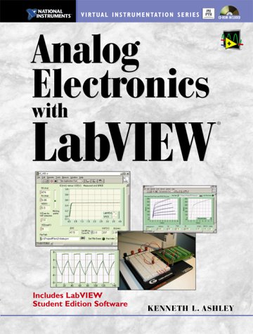
Kenneth L. Ashley0130470651, 9780130470652
Table of contents :
Copyright……Page 8
National Improvements | Virtual Instrumentation Series……Page 9
Preface……Page 10
References……Page 12
Hardware and Software Requirements……Page 13
Unit 1. Elementary Circuit Analysis for Analog Electronics……Page 17
Figure 1.1. (a) Dc circuit for the basic NMOS amplifier. (b) Circuit for determining the gate voltage, VG…….Page 18
Figure 1.2. Circuit for illustrating the determination of the drain voltage, VD…….Page 19
Figure 1.4. Circuits for low (a) and high (b) frequencies…….Page 20
Unit 2. Transistors and Voltage Amplification……Page 23
Figure 2.4. Basic NMOS amplifier with resistor gate biasing and input signal Vs. (a) Complete circuit. (b) Signal (or ac or incremental) circuit. The signal circuit is obtained by setting the power supply (dc) node to zero volts. (c) Linear signal circuit replaces the linear schematic representation…….Page 25
2.2. Fundamentals of Signal Amplification: The Linear Circuit……Page 27
Figure 2.2. Basic linear model of a voltage amplification device. Model parameters are gm and rin…….Page 28
Figure 2.3. Basic linear model of a voltage amplification device with load RL connected…….Page 29
2.4. Transistor Output Resistance and Limiting Gain……Page 30
Figure 2.5. Basic linear circuit with transistor linear model. Circuit includes signal source voltage and load RL, Transistor model now includes output resistance rout…….Page 31
2.5. Summary of Equations……Page 32
Unit 3. Characterization of MOS Transistors for Circuit Simulation……Page 33
Figure 3.1. MOS transistor consisting of a metal – oxide – semiconductor layered structure (plus a metal body contact on the bottom). A positive gate voltage, VG > Vtno, induces a conducting channel under the oxide, which connects the two n regions, source and drain. All voltages are with respect to VB, that is, the body (substrate) of the transistor. (a) No channel; (b) uniform channel; (c) channel is just pinched off at the drain end of the channel; (d) channel length is reduced due to drain pn-junction depletion region extending out along the channel…….Page 34
Figure 3.2. Common-source circuit configuration for discussion of the dc model parameters of the NMOS transistor. The three-terminal transistor symbol implies that the body and source are connected…….Page 36
Figure 3.3. Mathcad-generated output characteristic for the NMOS transistor. The plot illustrates the linear and active regions. The linear region is also called the triode region or presaturation region. Current is in microamperes and Veffn = 0.8 V. Also plotted is the ideal characteristic with zero slope in the active region…….Page 37
Figure 3.4. NMOS transistor circuit with a resistor, RS, in the source branch. With the body attached to VSS, VSB = IDRS…….Page 41
Figure 3.5. Diagrammatic NMOS transistor biased into the linear region…….Page 44
3.5. Summary of Equations……Page 45
4.1. Amplifier Circuit and Signal Equivalent Circuits……Page 46
Figure 4.1. (a) Ideal NMOS in a basic common-source amplifier circuit (output, Vocs). Dc supply nodes of Fig. 4.1(a) are set to zero volts to obtain the signal circuits of Fig. 4.1(b) and (c). An alternative output is Voef [shown in (b)], which is the source-follower amplifier stage. Voltage variable Vg is the input for both cases…….Page 47
Figure 4.3. (a) Linear model that includes all contributions to the signal drain current, Id, as given in (4.1). The body-effect parameter, gmb, is a positive number such that current from the current source is in the direction opposite the arrow. (b) Current source of body effect is reversed to eliminate the minus sign, and a resistor replaces the gds current source…….Page 48
4.3. Transconductance Parameter……Page 49
4.4. Body-Effect Transconductance Parameter……Page 51
Figure 4.4. Signal circuit with the addition of a current source due to the body effect. In this example, Vb = 0 V and Vsb = IdRS…….Page 52
Figure 4.6. Signal circuit that includes addition of the output conductance. The equivalent resistance has magnitude 1/gds…….Page 53
Figure 4.7. Transistor output characteristics without and with input signal, Vg. A solution for the drain current and drain – source voltage in both cases is the intersection between the respective characteristics and the load line of the amplifier circuit…….Page 56
Unit 5. Common-Source Amplifier Stage……Page 58
Figure 5.2. A signal source is connected to the gate through a coupling capacitor. The capacitor is necessary to isolate the dc circuit from the signal source…….Page 59
Figure 5.4. Common-source amplifier stage signal circuit, with all dc nodes set to zero volts. The transistor model includes output resistance 1/gds, which appears directly in parallel with RD with the source grounded…….Page 61
5.3.1. Nonlinearity Referred to the Input……Page 64
Figure 5.5. Common-source amplifier stage output characteristics. Output characteristics are from top to bottom, large high-current signal swing, iDhi, dc bias, ID, low-current signal swing, iDlo. Also shown is the load line. The current – voltage circuit solution is always the intersection between a given characteristic and the load line…….Page 65
Figure 5.6. Dc circuit of the dual-power-supply common-source amplifier. The gate is at ground potential, allowing the signal to be connected directly to the gate. RG is necessary only to prevent shorting out the input signal…….Page 67
Figure 5.7. Amplifier circuit with a bypass capacitor attached between the source and ground to tie the source to signal ground. Signal input is attached directly to the gate. Body and source are connected internally in the project chip for the transistor used in the amplifier…….Page 68
Figure 5.8. Signal circuit for dual-power supply common-source amplifier. Input signal voltage, Vi, is divided between Vgs, the control voltage, and the source resistor according to the ratio 1: gmRS…….Page 69
Figure 5.9. NMOS common-source amplifier with RS for bias and gain stabilization. Gate bias is provided by a voltage-divider network consisting of RG1 and RG2. The body and source terminals are connected…….Page 70
Figure 5.10. Output characteristic of the transistor of the amplifier with bias VDS set approximately according to (5.22). The signal is restricted within the range VDD – VRS and approximately veffn. The characteristic curves are for no signal (solid plot) and for the signal at a maximum (dashed plot), as limited by the transistor going into the inactive (linear) region. The load lines are dc (solid line) and signal (ac, dashed line)…….Page 72
Figure 5.12. Computed maximums for negative and positive output voltage signal peaks as a function of VG: Vdplus, positive maximum; Vdminus, negative maximum…….Page 74
5.7. Exercises and Projects……Page 76
Figure 6.1. Circuit with coupling capacitor. Capacitor blocks the signal at low frequencies. Cg and RG = RG1 || RG2 must be selected for | XCg | Data Acquisition>>Analog Input>> AI Acquire Waveform.vi. Go to Options in the Functions Tool Bar to Change Palette Set if desired…….Page 183
Figure A.2. Front Panel of LabVIEW VI AI Acquire Waveform.vi. Digital Controls provide for various inputs including the number of samples to be taken, in this example, 1000. The output is the designated waveform and is an array of sample values of index 0 through 999 in this case…….Page 184
Figure A.4. LabVIEW VI Diagram with Sequence Structure. This Structure executes in order of index at the top of the Frames. Frame 1 shown contains the VI for reading voltage. Frame 0 contains the VI for sending voltage. Click on arrows to move through Frames. Also shown is the Structures Palette under Functions and the process of adding a frame…….Page 185
A.1.3. Programming Exercise: Digital Controls and Digital Indicators……Page 186
Figure A.6. Top Diagrams: Locating the value terminal on the icon and moving the Wiring Tool to the Digital Control terminal. Bottom Diagrams: Completed wiring for Frame 0 and Frame 1. Completion of Frame 1 is discussed below…….Page 187
Figure A.7. Diagram showing Frame 1. The VI Mean.vi has been added to average the data samples…….Page 189
Figure A.8. Front Panel with addition of a Waveform graph. The graph is obtainable from the Front Panel under Controls>>Graph>>Waveform Graph…….Page 190
Figure A.10. Y-scale Formatting showing the section of no grid from Grid Options. Selection of Digits of Precision is also made in this window…….Page 191
A.2. ADC and the Autoranging Voltmeter……Page 192
Figure A.12. Diagram of autoranging dc voltmeter, Voltmeter.vi. The While Loop runs until the comparison finds the measured value less than the lowest possible limit…….Page 193
Figure A.13. LabVIEW measurement of a sine-wave voltage with peak of 10 mV. The sinewave is sampled at two limit settings of (a) 100 mV and (b) 2 V. The resolutions are (a) 48.8 V and (b) 1.22 mV…….Page 194
Figure A.14. Front Panel for a possible LabVIEW oscilloscope. Digital Controls provide for inputs of Frequency, Count (number of samples), and #cycles. Digital Indicators show Samples/Sec, Sec/Sample, VDC, and Vac Peak. The limits are set in the Diagram…….Page 195
Figure A.16. DAC in the bipolar mode. Plot of the programmed voltage sent out (0.1-mV steps) versus measured actual output voltage. The graph on the right is a plot of the input voltage samples for a single output sweep…….Page 196
Figure A.17. The full range of the output sweep is 10 mV. (The X-axis is before the 100:1 voltage division.) The input channel has low resolution, as revealed by the steps in the plot…….Page 197
Figure A.18. (a) Chan0_in samples for a voltage in a plateau region in the plot of Fig. A.17. (b) Samples for a voltage from the transition region…….Page 198
Figure A.19. The Front Panel and Diagram of SR_A.vi. LabVIEW AO Write receives the array of the numerical values of the waveform and sends them out on the output channel. The oscilloscope is launched in sequence and measures the response voltage of the input channel while the output array is still being executed…….Page 199
Unit B. Characterization of the Bipolar Junction Transistor for Circuit Simulation……Page 200
Figure B.1. Diagrammatic pn-junction diode. Applied voltage VD is shown for forward bias for which current freely flows. Opposite polarity is reverse bias, where the diode is essentially cut off and ID = –IS…….Page 201
Figure B.2. Diagrammatic semiconductor pnp transistor. The input junction on the left has forward bias voltage VD, and the output junction on the right is shorted for zero bias. The input pn-junction diode current ID couples with the output pn junction to flow into the output p region…….Page 203
Figure B.3. Diagrammatic semiconductor pnp transistor in active-mode operation. Regions are now designated emitter, base, and collector. The emitter – base junction is forward biased and the collector – base junction is reverse biased…….Page 204
Figure B.4. Amplifier circuit incorporating a pnp transistor. The output voltage is with respect to ground at the n-region terminal. The base is common to the input and output and hence, this is the common-base amplifier configuration…….Page 205
Figure B.5. Common-emitter transistor amplifier configuration. The common terminal is now the p-emitter region and the input is at the base (n region). The output is between the common emitter and the collector. This diagram includes a possible IB and thus IC < IE, as is discussed in Unit B.3…….Page 206
Figure B.6. Diagrammatic pnp structure showing the effect of base – collector voltage on base width…….Page 207
B.3. BJT Base, Emitter, and Collector Currents in the Active Mode……Page 208
Figure B.7. BJT (npn) in the common-base configuration, showing terminal voltages and branch currents…….Page 209
Figure B.8. Diodelike characteristics of the base currents. They are separately associated separately with their respective pn junctions. These currents do not couple across the base…….Page 210
Figure B.9. Circuit for measuring base current in the open-collector diode-connected circuit…….Page 213
Figure B.10. Circuit for measuring emitter current. In this circuit, VBC = 0 and (B.16) applies…….Page 214
Figure B.12. Circuit for measuring transistor output characteristic and DC versus IC…….Page 216
B.6. SPICE Solution for IC versus VCE of the Measurement Circuit……Page 220
B.7. Collector-Emitter Voltage and Collector Current in the Saturation Region……Page 223
B.8. SPICE BJT DC as a Function of Collector Current……Page 224
Figure B.14. LabVIEW computed plots of IC(mA) and IB(mA) as a function of VBE(V), including components IB1 (ideal) and IB2 (leakage)…….Page 226
Figure B.15. LabVIEW measurement of ratio IC/IB = DC as a function of IC…….Page 227
B.9. Signal or Incremental Common-Emitter Current Gain……Page 228
B.10. Summary of Equations……Page 229
C.1. DC (Bias) Analysis……Page 230
C.1.1. DC (bias) Formulation……Page 231
Figure C.2. Linear signal model for the BJT. Model parameters are rb, r, gm, and ro. Added to the model are circuit components RC and applied voltage Vbe…….Page 233
Figure C.3. Transistor output characteristic with no signal and signal. Also plotted is the RC load line. The solution for iC and vCE is always the intersection…….Page 235
C.2.1. Determination of the Linear Model Parameters……Page 236
Figure C.4. Signal equivalent circuit for the amplifier. dc nodes have been grounded and the capacitor has been shorted…….Page 237
C.3.2. Overall Gain Magnitude from Signal Source Voltage to Output……Page 239
C.4. Accuracy of Transistor Gain Measurements……Page 240
C.5. Effect of Finite Slope of the Transistor Output Characteristic……Page 242
Figure C.6. Signal model of the circuit for the determination the characteristic frequency of the frequency response associated with the coupling capacitor…….Page 243
C.6.2. Coupling Capacitor for Measuring the Base Input Voltage……Page 245
Figure C.7. Common-emitter amplifier for measuring the amplifier gain as a function of bias current. The signal base – emitter voltage is measured at Vx…….Page 246
Figure C.8. Common-emitter amplifier with active (transistor) load. The npn is the driver transistor and the pnp is the load transistor. The input signal source could be moved to the base of the pnp, in which case the two transistors play opposite rolls…….Page 247
C.7.1. Gain of the NPN – PNP Common-Emitter Amplifier with Active Load……Page 248
Figure C.10. Amplifier with an emitter resistor in emitter branch of pnp to increase the output resistance at the collector of the pnp. Also included is a capacitor, Cb, for grounding (signal) the base voltage of the pnp…….Page 250
Figure C.11. Linear circuit for the determination of the output resistance at the collector for a circuit with emitter and base resistor…….Page 251
C.8. Frequency Response of NPN – PNP Amplifier Due to the Base Shunt Capacitor……Page 255
Figure C.12. Segment of the npn – pnp amplifier of Fig. C.10 showing the addition of a pnp base-bypass capacitor, Cb…….Page 256
Figure C.13. Mathcad-generated plots of the magnitude of Rop(f) using (57) and (61). The calculation made with the approximate form, (61), also uses the approximate forms for f2 and fz…….Page 258
C.9. Common-Emitter Stage with Emitter Resistor and the Emitter-Follower Amplifier Stage……Page 260
Figure C.15. Linear circuit for deriving the input resistance of the common-emitter stage with emitter resistor. The amplifier output nodes for the common-emitter stage (Voce) and the emitter-follow (Voef) stage are indicated…….Page 261
C.9.2. Emitter-Follower Amplifier Stage……Page 263
C.10. Summary of BJT Model Parameter Relations……Page 265
C.11. Summary of Circuit Equations……Page 266
C.11. Summary of Circuit Equations……Page 268
Laboratory Project 1. Basic Circuit Analysis for Electronic Circuits and Programming Exercises……Page 271
P1.1. Resistor Voltage-Divider Measurements……Page 272
P1.2. Resistor Voltage Divider with Current Measurement……Page 277
P1.3. Resistor Voltage Divider with Resistor Measurement……Page 279
P1.4. Resistor Voltage Divider with a Sine-Wave Source Voltage……Page 282
P1.5. Frequency Response of a Resistor-Capacitor Circuit……Page 283
P2.1. NMOS Common-Source Circuit with Drain Current Measurement……Page 285
P2.2. NMOS Common-Source Amplifier with Resistor Gate Bias Circuit……Page 289
P2.3. Amplifier with Signal and Gain Measurement……Page 291
P3.1. SPICE Parameters and Pin Diagram……Page 295
P3.2. SPICE Equations……Page 296
P3.4. Low-Voltage Linear Region of the Output Characteristic……Page 297
P3.5. PMOS Parameters from the Transfer Characteristic……Page 299
P3.6. PMOS Lambda from the Transfer Characteristic……Page 300
P3.7. PMOS Output Characteristic……Page 302
Laboratory Project 4. Characterization of the NMOS Transistor for Circuit Simulation……Page 304
P4.1. SPICE Parameters and Chip Diagram……Page 305
P4.3. SPICE Equations……Page 306
P4.4. NMOS Parameters from the Transfer Characteristic……Page 307
P4.5. NMOS Lambda from the Transfer Characteristic……Page 309
P4.6. NMOS Gamma SubVI……Page 310
P4.7. NMOS Gamma……Page 312
P4.8. NMOS Circuit with Body Effect……Page 313
P5.1. SPICE Equations and Pin Diagram……Page 315
P5.2. PMOS Common-Source Amplifier DC Setup……Page 316
P5.3. Amplifier Gain at One Bias Current……Page 318
P5.4. Amplifier Gain versus Bias Current……Page 319
P6.1. PMOS Schematic and Pin Diagram……Page 321
P6.2. SPICE PMOS and Circuit Equations……Page 322
P6.3. PMOS Current-Source Amplifier DC Setup……Page 323
P6.4. Amplifier Gain……Page 324
Laboratory Project 7. NMOS Common-Source Amplifier Stage with Source-Resistor Bias……Page 326
P7.2. NMOS Common-Source Amplifier DC Evaluation……Page 328
P7.3. Amplifier Gain at Optimum Bias for Linear Output……Page 330
P7.4. Optimum Bias Stability Test……Page 332
P7.5. Amplifier Frequency Response……Page 334
P8.1. SPICE Equations and Pin Diagram……Page 336
P8.2. Source-Follower DC Evaluation……Page 337
P8.3. Source-Follower Voltage Transfer Relation……Page 338
Laboratory Project 9. MOSFET Differential Amplifier Stage……Page 339
P9.1. SPICE Equations and Pin Diagram……Page 341
P9.2. DC Evaluation of the Single-Power-Supply Differential Amplifier……Page 342
P9.3. Determination of the PMOS Parameters……Page 344
P9.4. Amplifier Gain Measurement……Page 345
P9.5. Transistor Parameters and DC Imbalance……Page 347
Laboratory Project 10. Current Mirror and Common-Source Amplifier with Current-Source Load……Page 349
P10.1. SPICE Equations and Pin Diagram……Page 350
P10.2. Evaluation of the Current-Source Circuit……Page 351
P10.3. Evaluation of the Mirror-Current Circuit……Page 352
P10.4. Evaluation of the Bias Setup……Page 353
P10.5. Measurement of the Amplifier Gain versus Drain Current……Page 354
P11.1. SPICE Equations……Page 356
P11.2. Bias Circuit Setup……Page 357
P11.3. Opamp Offset Voltage……Page 359
P11.4. Evaluation of the Bias Balancing Circuit……Page 360
P11.5. Evaluation of the Gain and Signal Limits with Swept Input……Page 361
P11.6. Evaluation of the Gain with Sine-Wave and Square-Wave Signals……Page 363
Laboratory Project 12. Operational Amplifier Integrator and Oscillator……Page 364
P12.1. SPICE Equations……Page 365
P12.2. Opamp Integrator……Page 366
P12.3. Opamp Oscillator……Page 368
Laboratory Project A. Communicating with the Circuit Board Using the DAQ……Page 371
PA.1. Sending and Receiving Voltages with the Sending and Receiving VIs……Page 372
PA.2. Sending and Receiving Voltages from the Front Panel……Page 373
PA.3. Plotting Measured Samples……Page 374
PA.4. Using the Autoranging Voltmeter……Page 376
PA.5. Observing the Oscilloscope Output Graph……Page 377
PA.6. Discrete Output Voltage from the DAQ……Page 378
PA.7. Discrete Input Voltage from the Circuit Board……Page 380
Laboratory Project B. Characterization of the Bipolar Junction Transistor for Circuit Simulation……Page 381
PB.2. SPICE Equations……Page 383
PB.3. Diode-Connected Transistor Measurements……Page 385
PB.4. Measurement of DC versus the Collector Current……Page 388
PB.5. BJT Output Characteristic Measurement……Page 392
PB.6. Simulation of the Output Characteristic Measurement……Page 393
PC.1. SPICE Equations and Pin Diagram……Page 395
PC.2. DC Circuit Setup and Parameter Determination……Page 396
PC.3. Amplifier Gain at One Bias Current……Page 397
PC.4. Amplifier Gain versus Bias Current……Page 399
Laboratory Project C2. NPN – PNP Common-Emitter Amplifier with Current-Source Load……Page 401
PC.6. SPICE Equations and Pin Diagram……Page 402
PC.7. Measurement of the PNP Parameters……Page 403
PC.8. DC Circuit Setup……Page 405
PC.9. Measurement of the Amplifier Gain……Page 408


Reviews
There are no reviews yet.