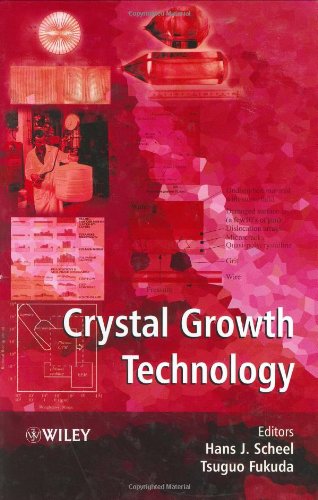
Hans J. Scheel, Tsuguo Fukuda0471490598, 9780471490593, 0471495247, 9780471495246
The major industrial crystals are treated: Si, GaAs, GaP, InP, CdTe, sapphire, oxide and halide scintillator crystals, crystals for optical, piezoelectric and microwave applications and more.
Contains 29 contributions from leading crystal technologists covering the following topics: General aspects of crystal growth technology Silicon Compound semiconductors Oxides and halides Crystal machining Epitaxy and layer deposition
Scientific and technological problems of production and machining of industrial crystals are discussed by top experts, most of them from the major growth industries and crystal growth centers.
In addition, it will be useful for the users of crystals, for teachers and graduate students in materials sciences, in electronic and other functional materials, chemical and metallurgical engineering, micro-and optoelectronics including nanotechnology, mechanical engineering and precision-machining, microtechnology, and in solid-state sciences.
Table of contents :
Crystal Growth Technology……Page 3
CONTENTS……Page 7
Contributors……Page 21
Preface……Page 27
PART 1: GENERAL ASPECTS OF CRYSTAL GROWTH TECHNOLOGY……Page 29
Abstract……Page 31
1.1 Historical Introduction……Page 32
1.2 The Development of Crystal-growth Methods……Page 33
1.3 Crystal-growth Technology Now……Page 38
References……Page 41
2.1 Introduction……Page 43
2.2.1 The Principle of Gibbs Free Energy Minimization……Page 44
2.2.2 Equilibrium Point-defect Concentration……Page 45
2.3.1 The Phase Transition……Page 47
2.3.2 Two-component Systems with Ideal and Real Mixing……Page 49
2.3.3 Phase Boundaries and Surfaces……Page 51
2.4.1 Mixed Crystals with Nearly Ideal Solid Solution……Page 53
2.4.2 Systems with Compound Formation……Page 56
2.4.3 Compositional Modulation and Ordering in Mixed Semiconductor Thin Films……Page 62
2.5.1 Driving Force of Crystallization……Page 64
2.5.2 Growth Mode with Two-dimensional Nucleation……Page 67
References……Page 68
Abstract……Page 71
3.1 Introduction……Page 72
3.2.1 Mathematical Formulation……Page 74
3.2.2 Numerical Technique……Page 79
3.3.1 Effect of Operating Parameters on Facetting……Page 80
3.3.2 Interaction between Melt Flow and Facet Formation……Page 83
3.3.3 Transparent Crystalline Phase……Page 88
3.3.4 Positioning of Facets along the Interface……Page 89
3.4 Conclusions……Page 90
Acknowledgments……Page 92
References……Page 93
4.1 Introduction……Page 97
4.2 Origin and Definitions of Striations……Page 98
4.3 Homogeneous Crystals with k(eff) 1……Page 102
4.4 Segregation Phenomena and Thermal Striations……Page 104
4.5 Growth of Striation–Free KTN Crystals……Page 110
4.6 Alternative Approaches to Reduce Striations……Page 112
References……Page 117
5.1 Introduction……Page 121
5.2.1 Theoretical Background……Page 122
5.2.2 High-resolution X-Ray Diffraction Experiments: A Five-crystal X-Ray Diffractometer……Page 124
5.3 Evaluation of Crystalline Perfection and Characterization of Crystal Defects……Page 128
5.4 Accurate Determination of Crystallographic Orientation……Page 132
5.5 Measurement of Curvature or Bending of Single-crystal Wafers……Page 136
5.6 Characterization of Process-induced Defects in Semiconductors: Implantation-induced Damage……Page 138
References……Page 140
6.1 Introduction……Page 143
6.2.1 Governing Equations……Page 144
6.2.2 Boundary Conditions……Page 146
6.3.1 Numerical Methods……Page 149
6.3.2 Software: Commercial versus Research, General versus Specialty……Page 150
6.4.1 Can we still Learn from a 1D Model?……Page 151
6.4.2 Is 2D Modeling Routine and Accurate?……Page 153
6.4.3 When are 3D Models Necessary?……Page 157
Acknowledgments……Page 163
References……Page 164
7.1 Introduction……Page 167
7.2 Magnetic Fields Applied to Czochralski Growth……Page 168
7.3 Numerical Modeling……Page 169
7.4 Vertical Magnetic Field (VMF)……Page 171
7.5 Cusp-shaped Magnetic Fields (CMF)……Page 175
7.7 Summary……Page 178
Acknowledgment……Page 179
References……Page 180
8.1 Introduction……Page 183
8.2 Technologically Important Hydrodynamics Processes during Crystal Growth……Page 185
8.3 Benchmark Problem……Page 186
8.4 Hierarchy of the Models and Codes and Summary of Benchmark Exercises……Page 190
8.5 Gravity-driven Convection Instability and Oscillations in Benchmark Configuration……Page 200
8.6 Convective Interaction and Instabilities in Configuration of Industrial GaAs Czochralski Growth……Page 201
8.6.1 Axisymmetrical Approach: Nonlinear Coupling Fluid Flow and Control Possibilities……Page 202
8.6.2 Three-Dimensional Analysis……Page 204
8.7 Conclusions……Page 209
References……Page 210
PART 2: SILICON……Page 215
9.1 Introduction……Page 217
9.2 Oxygen Behavior in Boron-doped Silicon Melts……Page 218
9.2.1 Oxygen Solubility in Silicon Melt……Page 219
9.2.2 Fused Quartz Dissolution Rate in Silicon Melts……Page 224
9.2.3 Evaporation from Free Surface of Boron-doped Silicon Melts in Fused-quartz Crucible……Page 228
Acknowledgments……Page 231
References……Page 232
10.1 Background……Page 233
10.2 Observation Methods……Page 234
10.3 Characterization……Page 237
10.4 Generation Mechanism……Page 241
10.5 Elimination……Page 243
10.6 Oxide Defect Generation……Page 244
10.7 Concluding Remarks……Page 247
References……Page 250
11.1 Introduction……Page 253
11.1.3 The Precipitation of Oxygen……Page 254
11.2.1 The v/G Rule for the Type of Grown-in Microdefects……Page 255
11.2.2 Alternative Views to the v/G Rule……Page 256
11.2.3 Void Reaction Control……Page 257
11.2.4 Perfect Silicon……Page 258
11.3.1 ‘Tabula Rasa’ Silicon and the Suppression of Oxygen Precipitation in Low-Vacancy-Concentration Material……Page 259
11.3.3 Comparison of Conventional and Vacancy-Engineered Control of Oxygen Precipitation……Page 261
11.3.4 The Installation of Vacancy Concentration Profiles in Thin Silicon Wafers……Page 263
11.3.6 The Mechanism of the Vacancy Effect on Oxygen Precipitation……Page 264
11.4.1 Recombination Rate……Page 266
11.4.4 The Difference of Equilibrium Vacancy and Interstitial Concentrations……Page 267
11.4.5 Formation Energies……Page 268
11.4.7 Vacancy Binding by Oxygen……Page 269
11.5 Unified Schematic Pictures of Vacancy Control for Crystal Growth and Wafer Processing……Page 270
References……Page 276
12.1 Introduction……Page 279
12.2 Experiments……Page 282
12.3 Results……Page 284
12.4.1 Balance Equation……Page 286
12.4.2 Discussion of Voronkov’s Relation……Page 290
12.4.3 Interface-shape Formation……Page 291
References……Page 292
13.1 Introduction……Page 295
13.2.1 The Photovoltaic Effect……Page 296
13.2.2 Minority-carrier Lifetime, τ……Page 297
13.2.3 Light Absorption……Page 299
13.3 Silicon Source Materials……Page 300
13.4 Ingot Growth Methods and Wafering……Page 303
13.4.1 Single-crystal Growth……Page 304
13.4.2 Multicrystalline Growth……Page 305
13.5 Ribbon/Sheet Growth Methods……Page 307
13.6 Thin-Layer Growth on Substrates……Page 311
13.8 Future Trends……Page 313
References……Page 315
PART 3: COMPOUND SEMICONDUCTORS……Page 319
14.1.1 Historical Background……Page 321
14.1.2 The Importance of SI GaAs and its Performance……Page 323
14.2.1 The Principle of Modern LEC Technique……Page 325
14.2.2 Correlation between Heat Transfer, Thermomechanical Stress and Dislocation Density……Page 328
14.2.3 Dislocation Patterns……Page 331
14.2.4 Principles of Native-defect Control……Page 333
14.2.5 Carbon Control……Page 338
14.3.1 Vapour-pressure-controlled Czochralski (VCz) Method……Page 341
14.3.2 Fully-Encapsulated Czochralski (FEC) Growth……Page 343
14.3.3 Hotwall Czochralski (HWC) Technique……Page 344
14.4 Conclusions and Outlook……Page 345
References……Page 346
15.1 Introduction……Page 351
15.2 InP Crystal Growth by the VGF Method……Page 352
15.3.1 Growth of Undoped GaAs……Page 359
15.3.2 Growth of Si-doped GaAs Crystals……Page 363
15.3.3 Growth of Zn-doped Crystals……Page 364
15.4 CdTe Crystal Growth by the VGF Method without Seed Crystals……Page 365
15.5 ZnTe Crystal Growth by VGF without Seed Crystals using the High-pressure Furnace……Page 372
References……Page 374
16.2 Properties of III-V Materials……Page 377
16.3 Growth Technology of III-V Materials……Page 378
16.3.1 HB and HGF Techniques……Page 379
16.3.2 LEC Technique……Page 380
16.3.3 Vapor-pressure-controlled Czochralski (VCZ) Technique……Page 381
16.3.4 VB and VGF Techniques……Page 383
16.4 Applications and Requirements for GaAs Single Crystals……Page 384
16.5 Growth of Large Single Crystals……Page 385
16.6 Growth of Low-Dislocation-Density GaAs Crystal……Page 387
16.7 Control of Quality and Yield of GaAs Crystals……Page 389
16.7.1 Twinning……Page 390
16.7.2 Lineage……Page 392
16.8.1 Absolute Value of Resistivity……Page 393
16.8.2 Uniformity of Microscopic Resistivity……Page 394
16.10 InP……Page 395
References……Page 397
17.2 Phase Equilibria in the Cd–Te System……Page 401
17.3 Crystal Growth versus Cd–Te Chemical Bond Characteristics……Page 405
17.4 Crystal Growth……Page 409
17.5 Bridgman Growth Modeling and Interface-shape Determination……Page 416
17.6.1 Properties at Macroscopic and Microscopic Scale……Page 421
17.6.2 Segregation……Page 422
17.7 Properties and Defects of the Crystals……Page 424
17.8 Purity, Contamination, Doping……Page 427
References……Page 428
PART 4: OXIDES AND HALIDES……Page 435
18.1 Introduction……Page 437
18.2 Phase-relation Study of LiTaO(3)……Page 438
18.2.1 Preliminary Studies by X-Ray Diffractometry……Page 439
18.2.2 Determination of the Congruently Melting Composition……Page 440
18.2.3 Optical Quality of the Congruent LiTaO(3)……Page 443
18.2.4 Conclusion……Page 445
18.3 Phase-relation Study of Bi(12)TiO(20)……Page 446
18.3.2 Lattice-constant Variations of the Bi(12)TiO(20) Phase……Page 447
18.3.3 New Phase Diagram……Page 450
18.3.4 Growth of Long Single Crystals……Page 452
18.4 Summary……Page 454
References……Page 455
19.1 Introduction……Page 457
19.2 LiTaO(3) for SAW Devices……Page 459
19.3 Langasite-family Crystals for Piezoelectric Applications……Page 462
19.4 Nonlinear-Optical Crystals for Blue SHG……Page 467
19.5 Summary……Page 469
References……Page 471
20.2.1 Growth of Large KDP (Potassium Dihydrogen Phosphate) Crystals of Improved Laser-damage Threshold……Page 473
20.2.2 Growth and Characterization of Organic NLO Crystals……Page 476
20.3.1 Growth and Optical Characterization of KTP (Potassium Titanyl Phosphate) Crystal [12–14]……Page 479
20.3.2 Growth and NLO Properties of Cesium Lithium Borate CLBO……Page 482
References……Page 486
21.1 Introduction……Page 489
21.2 Physical and Technical Aspects of the Direct Radio-frequency Melting in a Cold Container (Skull Melting)……Page 490
21.3 RF-furnaces for Zirconia Melting and Crystallization……Page 495
21.4 Phase Relations in Zirconia Solid Solutions. Y-stabilized (YCZ) and Partially Stabilized (PSZ) Zirconia……Page 498
21.5 Growth Processes of YCZ and PSZ Crystals……Page 500
21.6 Structure, Defects, and Properties of YCZ and PSZ Crystals……Page 503
21.7 Applications of YCZ and PSZ Crystals……Page 507
21.8 Conclusion……Page 510
References……Page 512
22.2 Crystal-growth Installation……Page 515
22.3 Growing of Crucibles……Page 516
22.4 Growth of Complicated Shapes……Page 520
22.5 Dice……Page 522
22.6 Group Growth……Page 524
22.7 Local Forming……Page 526
22.8 Sapphire Products for Medicine……Page 527
22.9 Improvement of Structure Quality of Profile Sapphire……Page 530
References……Page 537
23.2.1 R&D for Halogenide Crystal Perfection……Page 539
23.2.2 Traditional Crystal Growth Methods……Page 541
23.2.3 Automated Growth Principles and Technique……Page 542
23.3.1 Principles of the Method……Page 545
23.3.2 The Method Model and the Process Control Parameter……Page 546
23.4 Experimental and Practical Method Realization……Page 549
23.5.1 Activated Scintillators……Page 552
23.5.2 Undoped Scintillators……Page 553
References……Page 555
PART 5: CRYSTAL MACHINING……Page 557
24.1 Introduction……Page 559
24.2 Geometrical Parameters……Page 560
24.3 Survey on Slicing Methods for Silicon Single Crystal……Page 561
24.4 Material-removal Process……Page 565
24.5 General Comparison of Different Slicing Methods……Page 569
24.6 Surface Damage……Page 570
24.7 Economics……Page 572
24.8 Crystal Orientation……Page 576
References……Page 585
25.2 Crystals……Page 589
25.3 Machine-tools and Diamond Cutting Disks……Page 593
25.4.1 Traveling (Setting) Reference Base……Page 595
25.4.3 Positioning Tools……Page 596
25.4.4 Inspection Tools……Page 601
25.5 Tools for Lapping and Polishing Operations……Page 603
25.6 Optical Method for Inspection of Crystal Residual Stresses……Page 606
References……Page 613
26.2 Concepts of Plasma-CVM……Page 615
26.3 Applications of Plasma-CVM……Page 616
26.4.1 Slicing Machine……Page 617
26.4.2 Slicing Rate……Page 618
26.4.3 Kerf Loss……Page 619
26.4.4 Slicing of Silicon Ingot……Page 620
26.5.1 Planarization Machine……Page 622
26.5.2 Machining Properties……Page 623
26.6.1 Numerically Controlled Plasma-CVM System……Page 626
26.6.2 Machining Properties……Page 629
References……Page 633
27.2 Features and Performances……Page 635
27.3.1 General View……Page 638
27.3.2 Process Simulation and Results……Page 639
27.4.2 Numerically Controlled Stage System……Page 642
27.4.3 EEM Heads……Page 643
27.5.2 Software for Calculating Scanning Speed……Page 645
27.5.3 Performances of Numerically Controlled Processing……Page 646
27.6 Conclusion……Page 647
References……Page 648
PART 6: EPITAXY AND LAYER DEPOSITION……Page 649
28.1 Introduction……Page 651
28.2 Seven Epitaxial Growth Modes and the Role of Growth Parameters……Page 652
28.3 Control of Growth Modes……Page 663
28.4 Conclusions……Page 669
References……Page 670
29.1 Introduction……Page 673
29.2.2 Utilization of Rotary Electrode……Page 674
29.3 Experimental……Page 675
29.4.2 Electrical and Optical Properties……Page 676
References……Page 679
Index……Page 681


Reviews
There are no reviews yet.